
PowerScale: Best Practices for Semiconductor EDA Design Environments
Overview
Overview
-
This section describes the overall chip design workflow to help readers understand at a high-level stages of chip design. Understanding this workflow and the associated infrastructure to identify challenges that undermine the performance, efficiency, and scalability requirements for chip design. Historically, the EDA workflow is described, at a very high level, as consisting of the Front-end and Back-end flows though it is not uncommon for the flow to be broken into several high-level phases as shown in the figure 4 below. With each phase there are multiple EDA tools used for each phase by different role of designers.
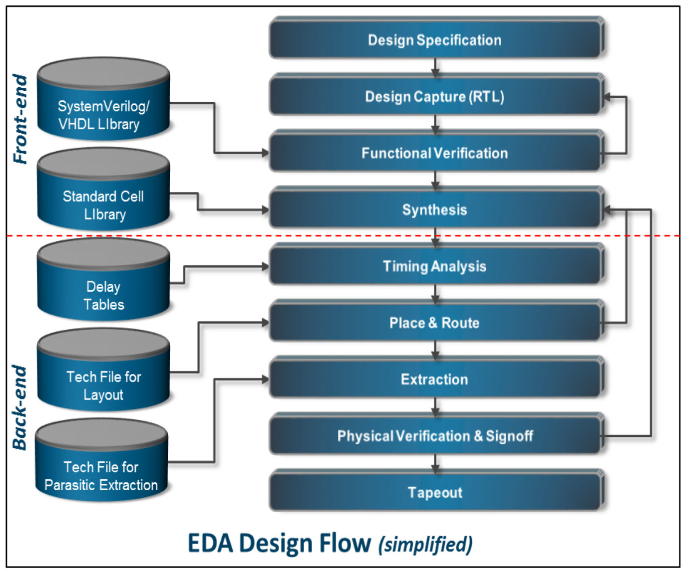
Figure 4. EDA Design Flow